RESEARCH
Summary
Micro-/Nanostructured surfaces express a variety of physical functionsinteracting with light, thermal fluid, force, electron, chemicals, and biological materials.
We develop high-efficiency manufacturing methods using laser or powders for these functional surfaces but also their novel applications.
We also study data-driven Process Informatics, to efficiently open the process windows of the laser/powder processes having complex physical phenomena.
Keywords; Micro-/nanostructure, surface, manufacturing, laser, powder, Process Informatics
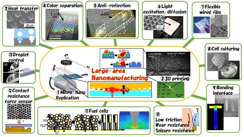
Schematic of manufacturing method using laser or powders and functional applications with micro-/nanostructured surfaces.
List of research topics
① Laser-assisted roller thermal nanoimprinting
② In-situ monitoring of selective laser melting (SLM) and its Process Informatics
③ Heat transfer surface of Micro/Nano hybrid structures
Roller imprinting of large-area micro/nanostructured optical devices; ④color separaters, ⑤anti-reflection/⑥excitation structures
⑦ Flexible wired films fabricated by screen printing of metallic nano particles
⑧ Injection molding of 3D cell culturing template
⑨ Bonding mechanism of anchoring and chemical-bonding effects
⑩ anomanufacturing of high-performance tribological surface; low friction, wear resistance, seizure resistance
⑫Small force sensor using contact resistance of nanostructured surface
⑬ Droplet sliding mechanism on texured surface
⑪ Controlled manufacturing of solid-oxide fuel cells
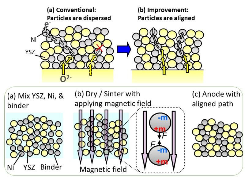
Fuel Cells have high generation energy which can be principally obtained from chemical energy of fuells to electric energy. This advantage accelerates researches and development because reduction of fuel cost and CO2 emission. Among the fuel cells, Solid Oxide Fuel Cells (SOFCs) performs the most highly because of the high-temperature operation. Furthermore, not only hydrogen but also hydrocarbon and alcohol can be directly used in SOFCs.
However, the microstructure is randomly located in conventional electrodes of SOFCs and oxygen ions, electrons, and gases transferred with high resistances. In anode, oxygen ions, electrons, gases are transferred in YSZ(Yttria-Stabilized Zirconia), Ni, pores, respectively, and they electrochemically reacted each other at their triple-phase boundaries (TPBs). In this study, Ni is aligned by magnetic field and the tortuosities (how hard to transfer) of the three phases are decreased and active TPB ratio could be increased.
K. Nagato, K. Shintani, T. Shimura, N. Shikazono, M. Nakao, “Magnetic alignment of anode structure in solid oxide fuel cell”, J. Electrochem. Soc. 166 (2019) F144-F148.
T. Shimura, K. Nagato, N. Shikazono, “Evaluation of electrochemical performance of solid-oxide fuel cell anode with pillar-based electrolyte structures”, Int. J. Hydrogen Energy 44 (2019) 12043-12056.
Laser-assisted nanoimprinting
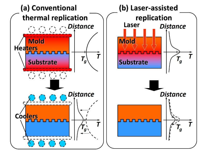
Conventional thermal nanoimprinting use more than enough energy. To replicate nanostructures on the surface of substrate, only surfaces of the mold and substrate have to be heated. I developed the laser-assisted nanoimprinting in which the mold surface is directly heated by laser and replicated nanostructures are cooled by the bases of mold and substrate after the laser is turned off. We prepare the mold with a quartz substrate as a transparent layer and a DLC thin film as a laser-absorption layer. Laser is irradiated to the DLC film through the quartz substrate and the surfaces of mold and substrate are heated, and immediately after the nanostructures are filled, they are cooled by the bases of the mold and substrate. We successfully replicated 100 nm pattern on glass and polymer surfaces with the time of several ms.
Keisuke Nagato, Yuki Yajima, Masayuki Nakao, “Laser-assisted thermal imprinting of microlens arrays –Effects of pressing pressure and pattern size–”, materials 12 (2019) 675. doi: 10.3390/ma12040675.
Keisuke Nagato, Nana Takahashi, Yuki Yajima, Masayuki Nakao, “Heat conduction and polymer flow in spot/scanning laser-assisted imprinting” Mech. Eng. J. 6 (2019) 18-00553. https://doi.org/10.1299/mej.18-00553
K. Nagato, K. Takahashi, T. Sato, J. Choi, T. Hamaguchi, M. Nakao, “Laser-assisted replication of large-area nanostructures”, J. Mater. Process. Technol. 214 (2014) 2444-2449. http://dx.doi.org/10.1016/j.jmatprotec.2014.05.025
Roller imprinting
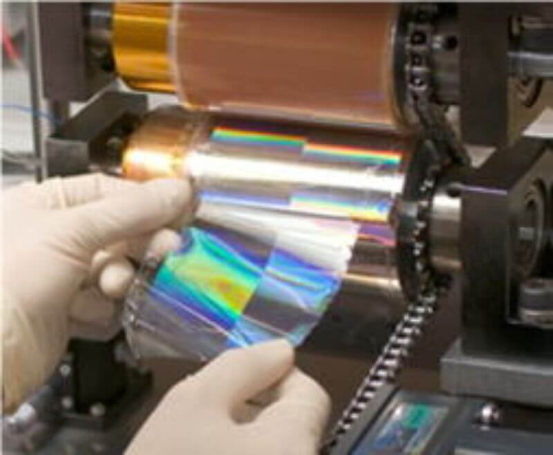
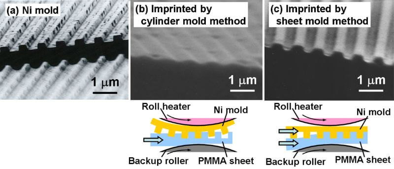
Polymer films, glass plates, and metal shhets are manufactured by continuous rolling.. Printing ink with roller is one of roller proceses. Nanoimprinting may be also carried out roller for lower-cost mass production. Furthermore, the advantages of roller molding are not only continuous process but also low partial touching, low pressure. For example, thin steel film can not be formed by stamping process because of drastically high friction between mold and substrate, but can be easily fomed by rolling process.
The figures below show continuous thermal imprinting with roller mold including heater. The polymer has to be heated / filled / cooled / demolded in turn. The right figure(b) shows a result with a cylinder mold method in which the Ni mold is covered and fixed to heater roller. In this case, the polymer that has been filled in nanostructured mold reflows and pattern reflows. On the other hand, when the mold and polymer sheet are got through by heater roller, the polymer can be demolded after cooled less than the glass transition temperature.
– K. Nagato, S. Sugimoto, T. Hamaguchi, M. Nakao, “Iterative roller imprint of multilayered nanostructures”, Microelectron. Eng., 87 (2010) 1543-1545.
Multilayered nanostructures
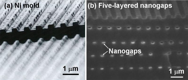
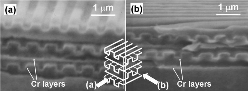
To fabricate three-dimensional photonic crystals or multi-layered optical device, the technique in which the nanostructures are piled up with a thickness corresponding the scale of nanostructures is nessesary. The left figure shows that the nanopores are periodically piled by repeating thermal imprinting and thermal bonding of PMMA thin films, The right figure shows that the Cr nanostructures are piled up by repeating thermal imprinting, depositing Cr, and thermal impringing. When the loading angle is changed, crossed nanostructures can beformed.
– T. Hamaguchi, H. Yonemoto, K. Nagato, K. Tsuchiya, T. Hamaguchi, M. Nakao, “Single-pass forming for three-dimensional microstructures by high-speed shearing of multilayered thin films”, J. Vac. Sci. Technol. B 26 (2008) 1771-1774.
– H, Suzuki, K. Nagato, K. Tsuchiya, T. Hamaguchi, M. Nakao, “Iterative imprint for multilayered nanostructures by feeding, vacuum forming, and bonding of sheets”, J. Vac. Sci. Technol. B 26 (2008) 1753-1756.
Heat-assisted injection molding
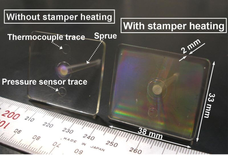
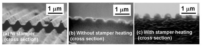
Nanoimprint lithography (NIL) is expected to be used for patterning thin resist mask on Si substrate etc., on the other hand, the nanoimprinting technique in which surfaces on bulk polymer or glass substrates for such as high-efficient optical devices, biodevices, or energy devices. Injection molding is one of most practical industrial technology which is widely used for various plastic parts of industrial machines because it has an advantage of three-dimensional featured parts with a mold (“cavity” in injection molding). Furthermore, melted polymer is injected in the cold mold, cooled and solidified at the same time, therefore, the cycle time can be shortened by nature. However, because the thermal flow rate from the hot polymer to the cold mold is high (because the thermal conduction of the metal mold is much higher than that of the polymer), the “skin layer”, i.e., solidified layr is formed and it is difficult to fill thin or nanostructured cavity. Optical disks such as CD, DVD, BD have nanostructured surface and replicated by injection compression molding with high-temperature mold, hish-speed injection, high-pressure compression, and using high-viscosity polymer.
I have proposed “heat-assisted injection molding (HAIN)”, in which the mold surface is kept more than glass transition temperature only during injection. Replica with conventional injection molding has poor replication, on the other hand, that with HAIN has good replication (following figures).
K. Nagato, “Injection compression molding of replica molds for nanoimprint lithography”, Polymers 6 (2014) 604-612. doi:10.3390/polym6030604
S. Hattori, K. Nagato, T. Hamaguchi, M. Nakao, “Rapid injection molding of high-aspect-ratio nanostructures”, Microelectron. Eng. 87 (2010) 1546-1549.
Past researches (~2009)
Gas cluster ion beam
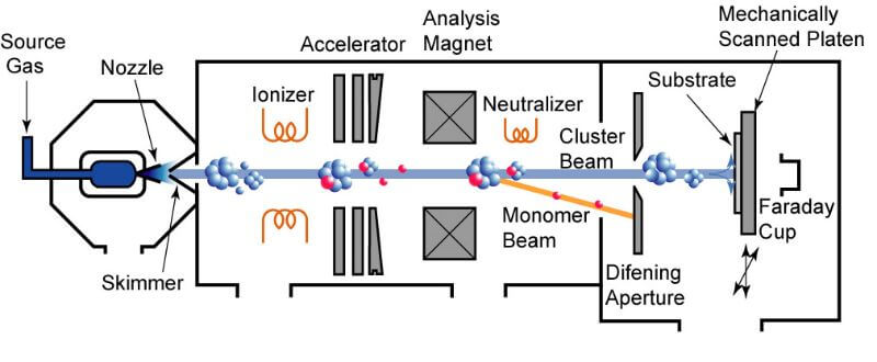
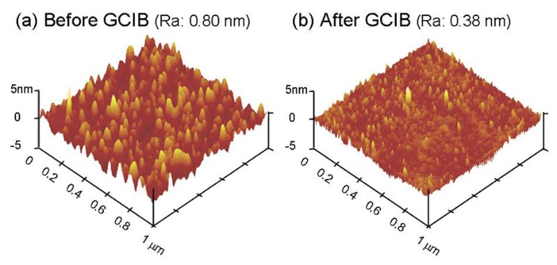
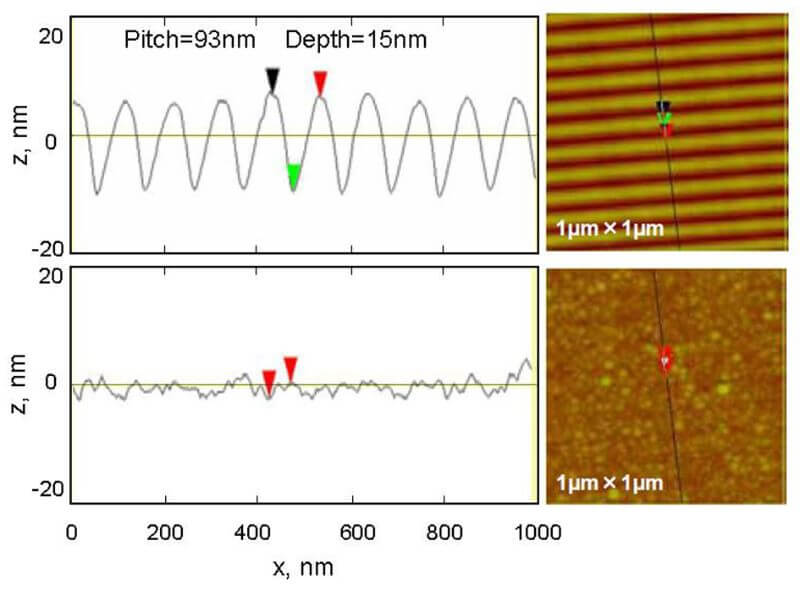
Patterned media as a next generation hard disk is inceasingly researched. Present miniturization technique of bit pitch is limited to achieve 1Tb/inch2 in recording density, i.e., the bit pitch is under 25 nm because the spins neighboring each other interfere and the recording cannot be kept. To overcome this problem, discrete track media(DTM) or bit-patterned media (BPM) in which the magnetic film is patterned. However, the patternd disk surface avoid the stable flyability of head. We proposed and developed that the trenches of magnetic film is refilled by nonmagnetic material (DLC, Cr, Pt, etc.).
We used gas cluster ion beam (GCIB) with a collaborator, Toyoda Lab., University of Hyogo. The surafece can be planarized by GCIB in dry condition. We obtained Ra2nm flat surface by irradiation of Ar cluster from L/S with a pitch of 90 nm and depth of 20 nm.
– K. Nagato, H. Tani, Y. Sakane, N. Toyoda, I. Yamada, M. Nakao, T. Hamaguchi, “Study of gas cluster ion beam planarization for discrete track magnetic disks”, IEEE Trans. Magn. 44 (2008) 3476-3479.
– N. Toyoda, K. Nagato, H. Tani, Y. Sakane, M. Nakao, T. Hamaguchi, I. Yamada, “Planarization of amorphous carbon films on patterned media using gas cluster ion beams”, J. Appl. Phys. 105 (2009) 07C127-1-3.
– N. Toyoda, T. Hirota, K. Nagato, H. Tani, Y. Sakane, M. Nakao, T. Hamaguchi, I. Yamada, “Planarization of bit-patterned surface using gas cluster ion beams”, IEEE Trans. Magn. 45 (2009) 3503-3506.
Atomchip
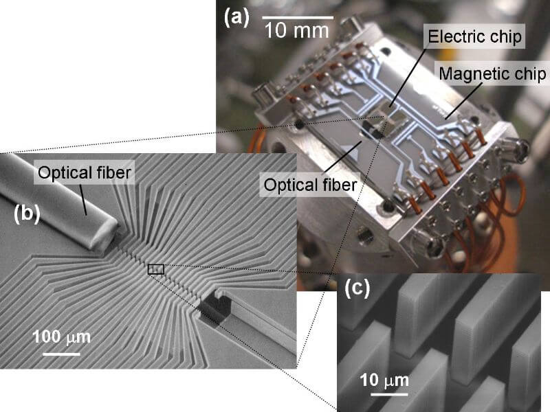
Atoms are cooled to ultralow temperature such as nK using lasers in a room temperature vacuum chamber. I collaborate with Katori Kab., The University of Tokyo and developing an atomchip on which laser-cooled atoms are manipulated on a chip and quantum information processing (QIP) is carried out. I fabricated the microelectrodes (left figure) using nano-/microfabrication technique (FIB, MEMS process, Laser) and actually seccessed thr electric trap. I also fabricated electrodes on which multi-atoms are trapped at trapsites or atoms are transfered.
– T. Kishimoto, T. Hachisu, J. Fujiki, K. Nagato, M. Yasuda, H. Katori, “Electrodynamic trapping of spinless neutral atoms with an atom chip”, Phys. Rev. Lett. 96 (2006) 123001-1-4.
– K. Nagato, T. Ooi, T. Kishimoto, H. Hachisu, H. Katori, M. Nakao, “Design and prototyping of Stark atom chip for electric trapping of laser-cooled atoms”, Precis. Eng. 30 (2006) 287-395.
Laser-assisted local synthesis single-walled carbon nanotubes
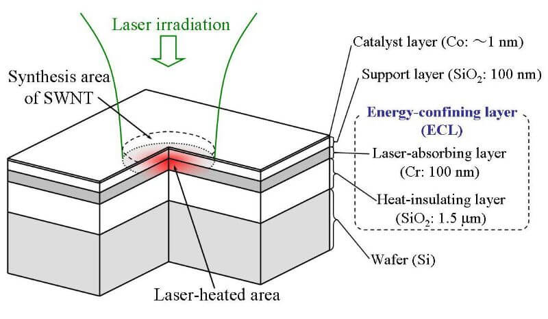
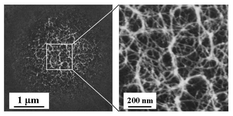
Single-walled carbon nanotubes (SWNTs) are promising candidate for new nanodevices such as single-electron FETs or high-performance gas sensors because of their unique electric, mechanical, and chemical characters. We developed a fabrication method that synthesizes SWNTs locally. Laser is irradiated on “energy-absorbing layer” and the surface with nano-particle catalysts at the irradiated region are heated locally. We successfully synthesized SWNTs in the area of 1 um (Left SEM images). It is dlarified SWNTs that is practical for electronic nanodevice by using Raman spectroscopy.
– K. Kasuya, K. Nagato, Y. Jin, H. Morii, T. Ooi, M. Nakao, “Rapid and localized synthesis of single-walled nanotubes by laser-assisted chemical vapor deposition”, 46 (2007) L333-L335.
Local synthesis of metal oxide nanowires
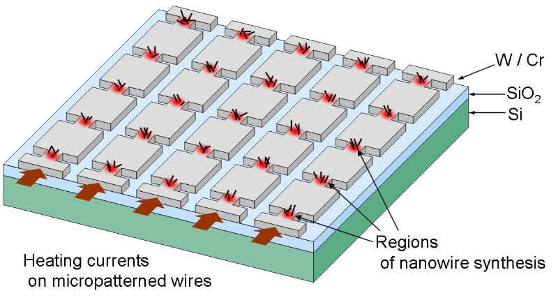
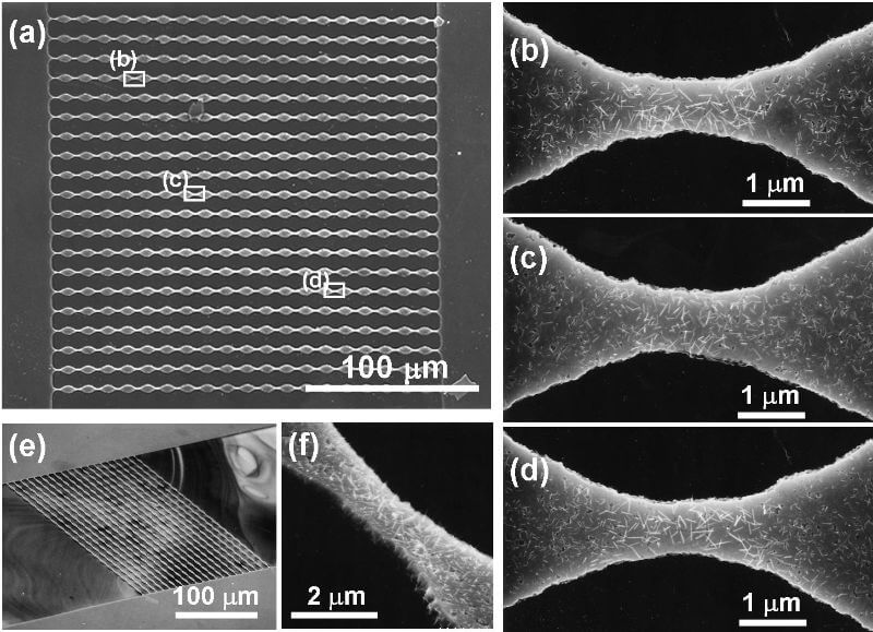
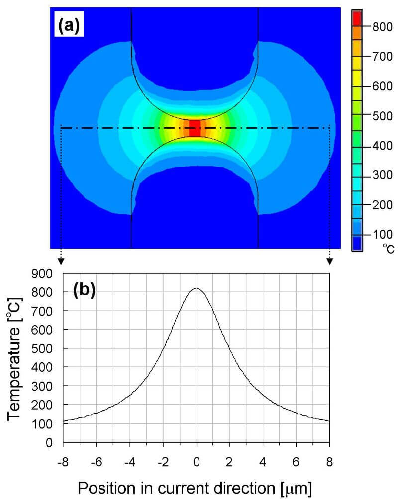
When some metal is heated under controlled oxygen atmosphere, single-crystal metal oxide nanowires are synthesized. The nanowires can be used for field-effect transistor (FET) or gas sensors because of their band gaps. They are also excepted to be probes od atmic force microscopy (AFM) or tips of field emission devices. The tungsten oxide (W18O49) nanowires were synthesized at the area arrayed periodic parts using patterned tungsten film. The narrow parts are locally heated by joule heating and nanowires are locally synthesized. This synthesis technique is practical to position control for device fabrication. Other metal oxide such as Fe2O3, Fe3O4, CuO nanowires can be synthesized by using simple annealing.
– Y. Kojima, K. Kasuya, T. Ooi, K. Nagato, K. Takayama, M. Nakao, “Effect of oxidation during synthesis on structure and field emission properties of tungsten oxide nanowires”, Jpn. J. Appl. Phys. 46 (2007) 6250-6253.
– K. Nagato, Y. Kojima, K. Kasuya, H. Moritani, T. Hamaguchi, M. Nakao, “Local synthesis of tungsten oxide nanowires by current heating of designed micropatterned wires”, Appl. Phys. Express 1 (2008) 014001-1-3.
– Y. Kojima, K. Kasuya, K. Nagato, T. Hamaguchi, M. Nakao, “Solid-phase growth mechanism of tugsten oxide nanowires synthesized from sputtered tungsten film”, J. Vac. Sci. Technol. B 26 (2008) 1942-1947.
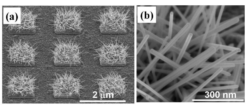
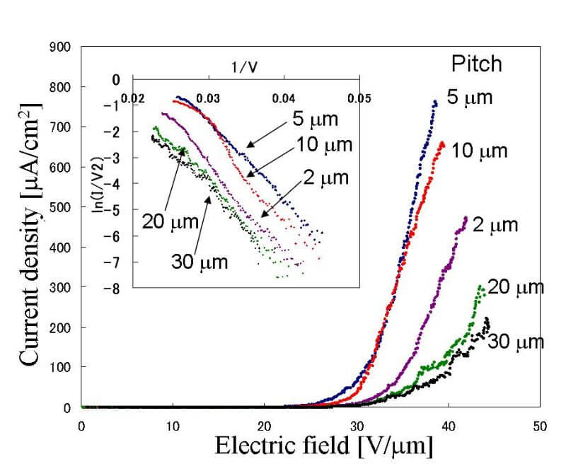
When the tungsten oxide nanowires are positioned at proper pitch, their field-emission properties can be optimized. When the pitch becomes wider, the electric fields at the apex of the nanowires become higher, on the other hand, when the pitch becomes narrower, the density of the islands of nanowires becomes higher and the current density per surface area becomes higher. We investigated the effect of pitch of nanowires on field-emission properties verifieng the pitches of island of tungsten (2/5/10/20/30um). It was found that the nanowires on the island with a pitch of 1 um (left figure) performed the highest current density.
K. Sekiya, K. Nagato, T. Hamaguchi, M. Nakao, “Morphology control of nickel oxide nanowires”, Microelectron. Eng. 98 (2012) 532-535.http://dx.doi.org/10.1016/j.mee.2012.07.049
M. Furubayashi, K. Nagato, H. Moritani, T. Hamaguchi, M. Nakao, “Field emission properties of discretely synthesized tungsten oxide nanowires”, Microelectron. Eng. 18 (2009) )1594-1596.
Antireflection nanostructure using Iron oxide nanowires
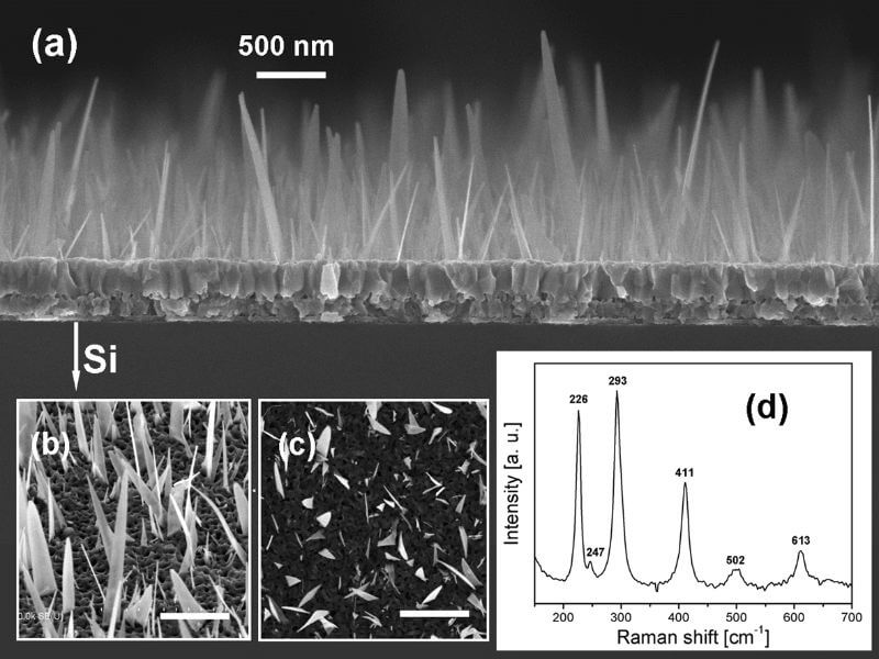
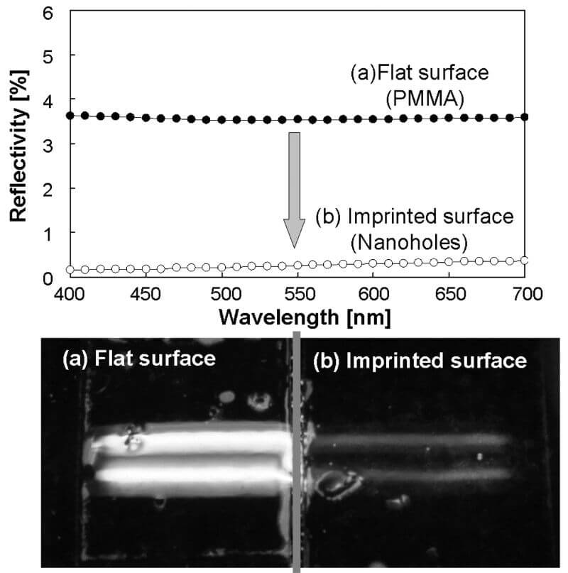
Antireflection nanostructure is expected to be used for high-performance displays or low-loss ollumination. Not only replication process such as nanoimprinting but also its fabrication of mold must be low cost. I proposed the shape-transfer method using a-Fe2O3 nanowires that can be fabricated by atmospeheric annealing of Fe as an initial structure. To transfer the shape of a-Fe2O3 nanowires to thick and conical, the nanowires are deposited Cr and then anisotropically etched. The surface of polymer which had been thermally imprinted by using this nanostructures as a mold performed low reflection ratio.
K. Nagato, H. Moritani, T. Hamguchi, M. Nakao, “Fabrication of antireflection-structured surface using vertical nanowires as an initial structure”, J. Vac. Sci. Technol. B 28 (2010) L39.
– K. Nagato, M. Furubayashi, T. Hamaguchi, M. Nakao, “Direct synthesis of a-Fe2O3 nanowires from sputtered thin film”, J. Vac. Sci. Technol. B 28 (2010) C6P11.
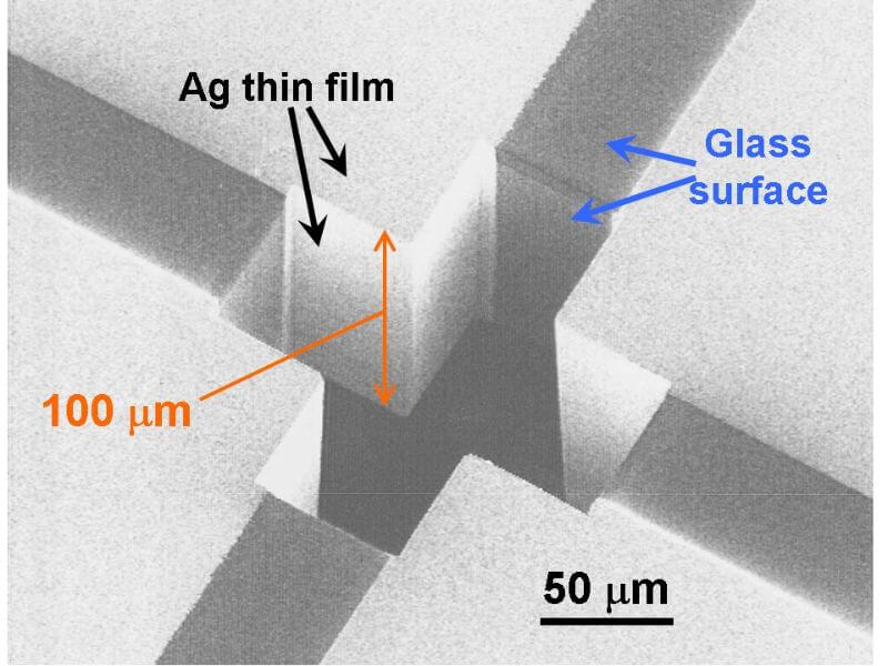
Automatic balancing system
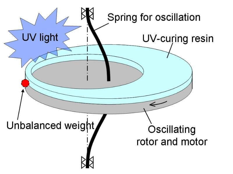
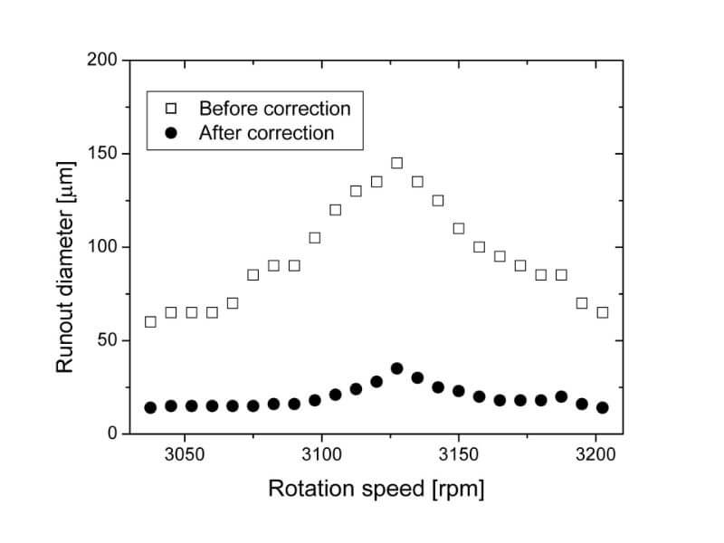
We proposed the automatic unbalance correction of rotors using symphathetic inversion. The high-speed rotors such as hard disks and polygon motors have to to be corrected precisely immediate after fabrication. We demonstrated the correction of the unbalance to 20% of original unbalance using a phenomenon that the UV-curing polymer in fluid with the center of the rotor positions at the inversion of the umbalance more than the rotation speed of resonance of the spring-mass system.
K. Nagato, T. Ide, N. Ohno, M. Nakao, T. Hamaguchi, “Automatic unbalance correction of rotors by synpathetic phase inversion of UV-curing resin”, Precis. Eng. 33 (2009) 243-247.